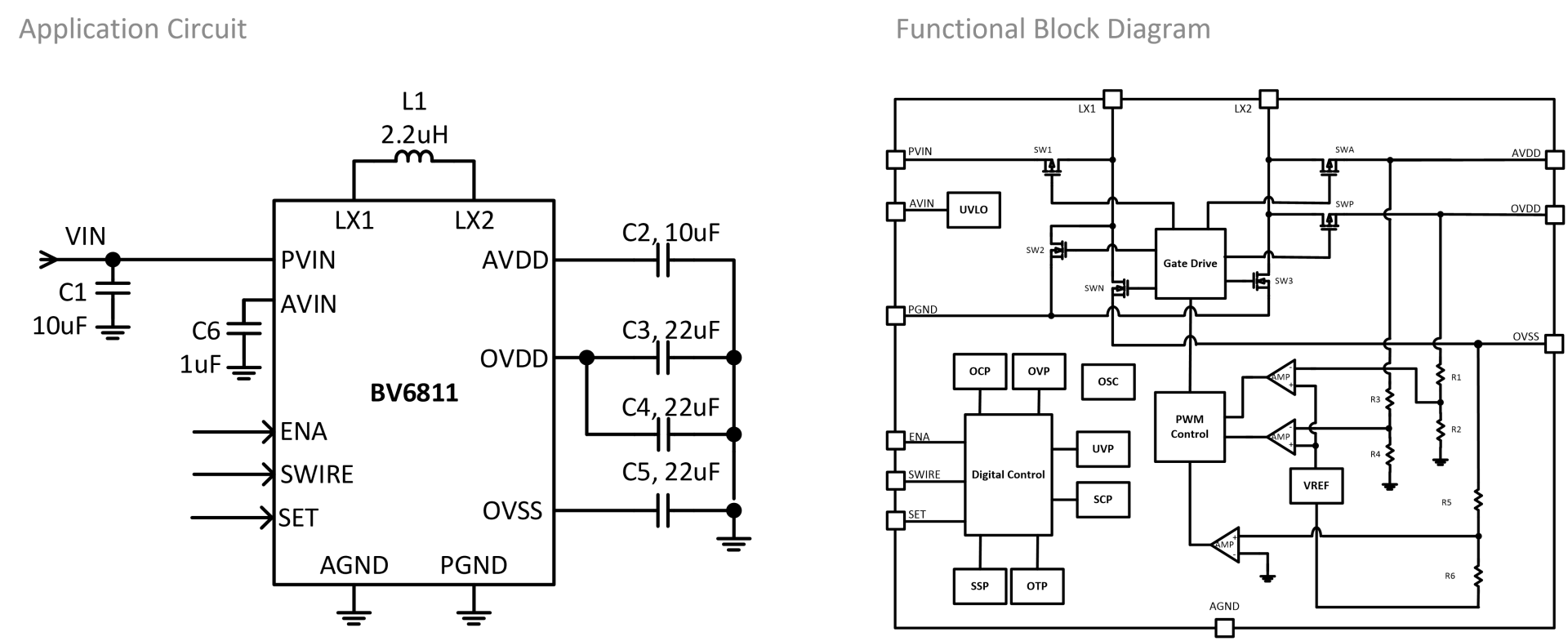
BV6811 does not need an extra charge pump circuit to generate the negative voltage output so that external capacitors required by the charge pump circuit can be eliminated and the PCB space can be achieved with very small.
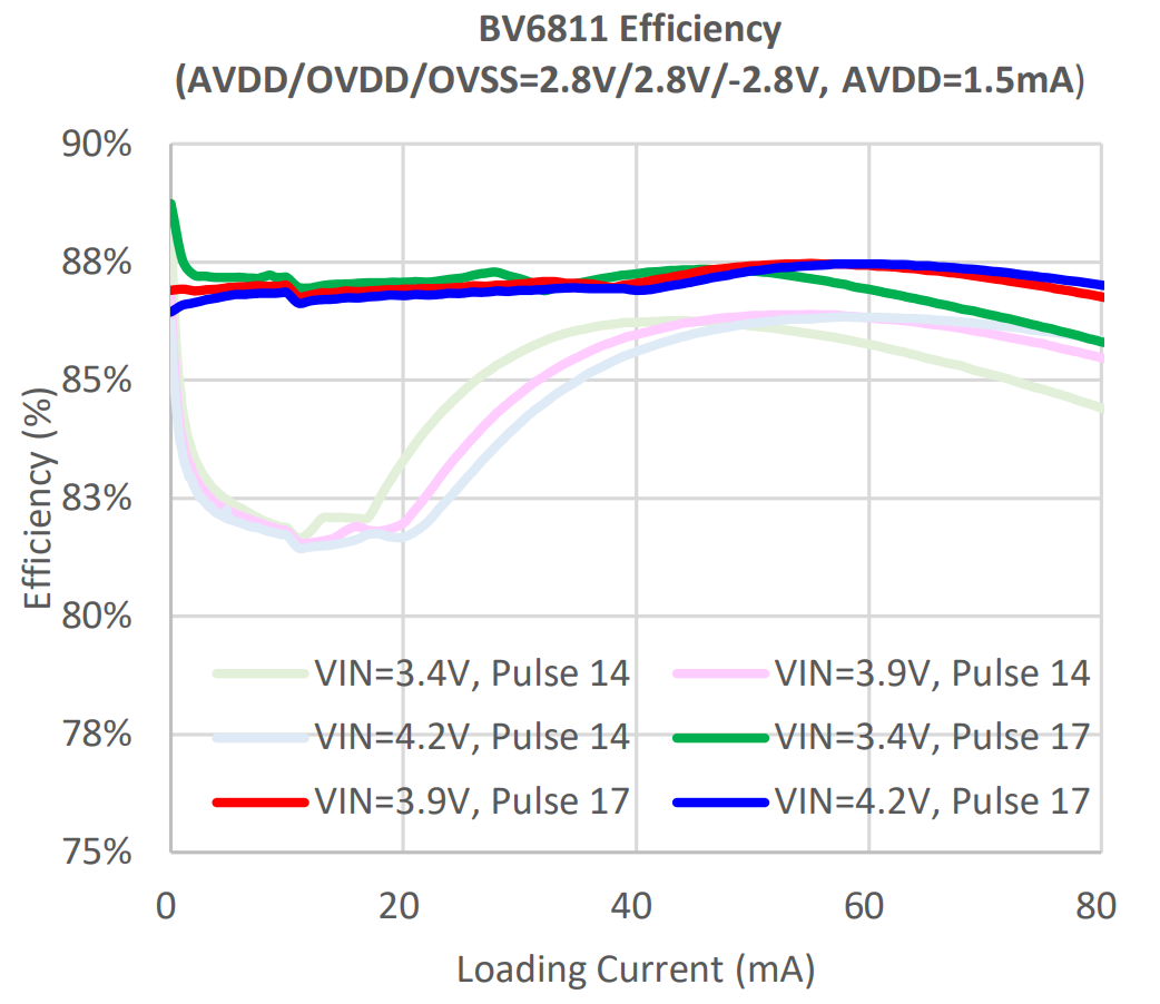
The output voltages can be adjusted by SWIRE pin. Compared with the scheme of generating negative voltage by a charge pump circuit, the best energy conversion efficiency can only be obtained near the negative voltage ratio provided by its charge pump circuit. This SITO architecture can provide a stable high conversion efficiency throughout the entire negative voltage adjusting range. Therefore, this solution can provide the optimal negative voltage output value according to different brightness requirements to reduce the power consumption of the AMOLED display significantly. This is the best solution that can optimize the solution form factor as well as display power consumption.
With its input voltage range from 2.7V to 5.5V, BV6811 is optimized for products powered by single-cell batteries with output currents up to 80mA. The BV6811 is available in the WL-CSP-12B 1.39mm x 1.64mm package.
- Single-inductor, Tripolar-output Topology
- Input Voltage Range: 2.7V to 5.5V
- Positive Output Voltage AVDD: 2.8V to 3.7V (Default is 3.3V±1%)
- Positive Output Voltage OVDD Range: 2.6V to 5.3V (Default is 3.3V±1%)
- Negative Output Voltage OVSS Range: -0.6V to -4.7V (Default is -3.3V±1%)
- 2.1MHz switching frequency with CCM, DCM and PSM
- Low Quiescent Current: 23μA
- AVDD Max. Loading is 20mA, OVDD and OVSS Max. loading is 100mA.
- Built-in Internal Soft start UVLO, UVP, SCP, OCP, OTP, and SSP protection
- Active Matrix OLED
- Portable Multi-Media Devices